Table of Contents >> Show >> Hide
The Sony Vaio P-series is the kind of laptop that makes people say, “Wait… they sold that in 2009?” It’s tiny, stylish, and weird in the best wayan 8-inch ultrawide display, a compact keyboard, and that “pocket computer” energy that modern laptops rarely bother with. The problem is that time has not been kind to aging storage, scarce replacement parts, and proprietary connectors.
The good news: you can revive a Vaio P without turning it into a tragic “retro shell with random modern parts hot-glued inside.” KiCad 7 introduced Background Bitmaps (reference images in the PCB editor), which lets you drop high-quality photos or scans of an original board into the layout canvas, then trace the outline, holes, and connector locations directly on top. That’s a huge advantage when the goal is a replacement board that actually fits the chassis and meets the existing cutouts.
Why the Vaio P Is Still Worth the Effort
Even critics who called the Vaio P slow couldn’t deny the charm: the high-resolution 1600×768 8-inch display and the ultra-portable form factor were genuinely distinctive. That uniqueness is exactly why it’s a great “revival” target today. You’re not trying to beat a modern ultrabook on benchmarks; you’re trying to keep an iconic chassis, keyboard, and screen usefulas a writing machine, a portable terminal, or a modern cyberdeck-style daily companion.
But retro laptop revivals usually hit the same wall: mechanical fit. The board has to match screw posts, shielding, port openings, and flex-cable geometry. Background bitmaps help you inherit the original board’s physical layout while changing the electronics underneath.
What “Background Bitmaps” Are (And Aren’t)
KiCad’s Background Bitmaps feature was introduced to help users copy PCB traces and footprint layouts from an existing reference board. In the PCB editor, you can place an image into the canvas, move it, scale it, adjust opacity, and even associate it with a board layer so it shows/hides with that layer. Crucially, the image is not included in fabrication outputsit’s a design-time overlay.
Think of it as a drafting table lightbox:
- Great for: board outlines, mounting holes, connector placement, keep-outs, and “route roughly like the original.”
- Not magic for: fixing perspective distortion, measuring hidden internal layers, or guessing the schematic from vibes.
Choose a Revival Strategy
“Revive” can mean very different things. Pick the smallest goal that gets you a win.
Strategy A: Adapter boards (fast wins, fewer tears)
Design a small PCB that solves one problem while leaving the rest alonelike replacing a damaged power-input area, adapting a weird internal connector to something standard, or repositioning ports to match the case openings. Smaller boards are cheaper, easier to debug, and easier to iterate.
Strategy B: A full replacement board (the big swing)
If the original motherboard is dead or too impractical, you can build a new “main board” that fits the chassis and reuses the existing openings and peripherals. This is mostly a mechanical engineering challenge disguised as electronics, which is exactly why background bitmaps matter.
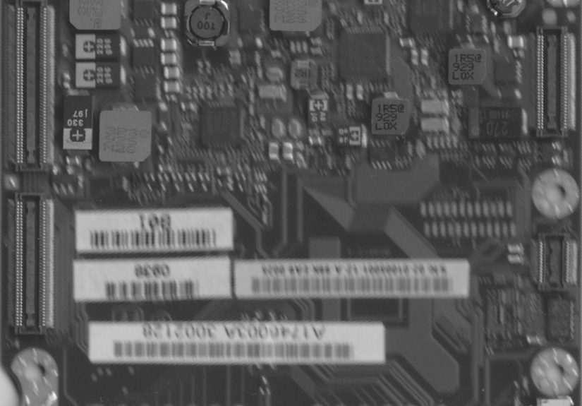
Capture and Prep Board Images
Your overlay will only be as accurate as your images. Aim for top-and-bottom images that are sharp, evenly lit, and as close to perfectly square as possible.
- Scanner: excellent sharpness and flat geometry, but watch out for tall components and accidental pressure damage.
- Camera/phone: safer for tall parts, but you must control perspective (tripod/stand, lens parallel to the board).
Before importing into KiCad, do a quick “image hygiene” pass in an editor (GIMP, Photoshop, etc.):
- Correct perspective so the PCB isn’t a trapezoid.
- Rotate until the board is truly level.
- Crop tightly to the PCB outline.
- Mirror the bottom image if your capture method flipped it.
Scaling tip: include a ruler in the shot, or at least measure a few distances (mounting-hole spacing, board width) with calipers. You’ll use these as anchors inside KiCad.
Overlay and Rebuild in KiCad
1) Add reference images
In the PCB editor, use the Add Image / Add Reference Image tool and place the top image. Add the bottom image too. You can move images with M, open their properties with E, and adjust opacity via the Appearance Manager so your new drawings don’t disappear under the photo.
2) Scale based on a known dimension
Scale the image using something measurable: the distance between two mounting holes is usually the most reliable. KiCad lets you scale by dragging image handles or by entering an exact scale factor in the image properties. Verify your scale with at least two measurements on opposite ends of the board to catch distortion early.
3) Tie images to layers (top vs. bottom)
Associate your top image with F.Cu and your bottom image with B.Cu. Now, when you flip the view to work on the other side, the correct image can appear. It’s a small trick with a big mental-health payoff.
4) Trace the mechanical skeleton
Start with the things that decide whether the board fits at all:
- Board outline on
Edge.Cuts - Mounting holes and alignment features
- Keep-outs for tall components, shields, hinges, and case ribs
If you want friendlier edges, use KiCad’s fillet tools to round corners instead of hand-drawing arcs.
5) Place the “hard anchors”
Next, place connector footprints directly over the bitmap: LCD, keyboard/trackpoint flex connectors, and anything that must line up with an external opening. This is where the overlay really shineswhen the pads line up, you’ve essentially “captured” the physical interface of the original motherboard.
A Vaio P-Focused Example Workflow
The Vaio P’s motherboard is compact and connector-dense, which makes it perfect for an overlay-first approach. A practical milestone is a mechanical replica PCB: a board that matches the original outline, holes, and connector locationseven if the electronics are still a placeholder. That single milestone unlocks everything that comes next.
Step-by-step milestone plan
- Import top and bottom images and set them to the appropriate layers.
- Scale using mounting-hole spacing, then sanity-check with board width.
- Redraw the outline on
Edge.Cuts. Add mounting holes. - Place the LCD connector footprint first and align it to the pads. If it matches, your scale is probably correct.
- Place the remaining flex and I/O connectors and check their alignment across the board.
- Add keep-outs where shielding cans or chassis ribs would collide with tall parts.
From there, you can choose your direction: design a new power-input section, build a keyboard/trackpoint interface board, or plan a complete modern mainboard. But you’ll be doing it on a PCB “frame” that already fits the Vaio P, rather than guessing in three dimensions like you’re playing hardware Jenga.
Mistakes That Waste the Most Time
- Assuming one measurement is enough: scale drift and distortion show up far from your chosen reference point. Verify multiple distances.
- Forgetting mirroring: bottom images are often reversed. Fix it before you commit geometry.
- Using the wrong connector footprint: similar-looking FPC connectors can have different pad styles and lock mechanisms. Confirm pitch and pin count.
- Letting images “steal clicks”: if you keep selecting the reference image while editing the outline, tweak selection filters so you can work without constant interruptions.
- Power improvisation: retro laptops may use unusual voltages and proprietary battery signaling. Don’t experiment casuallyespecially with lithium batteries. Safety first.
From KiCad to a Real PCB
Once your outline, holes, and connectors are correct, order a fit-check PCB: minimal copper, maybe no components, just enough to validate mechanical fit. If it mounts cleanly and the connectors land where they should, you’ve saved yourself from expensive revisions later.
To fabricate, you can export Gerbers and drill files from KiCad (then confirm them in a Gerber viewer), or use a service that accepts KiCad board files directly. Either way, treat the first run as an experiment: the goal is alignment and fit, not a perfect final motherboard on attempt one.
Experiences and Lessons From Builders
Required extra section (~): Builders who attempt a Vaio P revival with KiCad background bitmaps often describe the process as a mix of “surprisingly methodical” and “mildly haunted.” The tool makes the geometry approachable, but the workflow still teaches a few universal lessons.
The “photo reality check”
The first emotional speed bump is realizing that a “pretty good” photo isn’t good enough. Tiny perspective errors look harmless until you try to align a 0.5 mm pitch flex connector. That’s when the board turns into a funhouse mirror. Many builders end up taking multiple photo sets: one broad shot for outline and holes, and one close, high-resolution shot for each connector region. Stitching images or swapping overlays becomes normal. It’s not failureit’s calibration.
The satisfying moment: footprints snap into place
Once the images are clean and scaled, the workflow becomes weirdly satisfying. There’s a particular “yes!” moment when a connector footprint lands on the reference image and the pad row matches perfectly. At that point, the project stops being abstract. The board outline isn’t a guess anymore; it’s a traced fact. The connector location isn’t “roughly over there”; it’s locked to the original hardware. Makers often say that moment is what turns a scary rebuild into a solvable design exercise.
What people wish they did earlier
- Print a 1:1 paper mockup: exporting a PDF and checking it against the chassis (or the old board) catches scale mistakes quickly.
- Measure three things, not one: mounting-hole spacing, board width, and one connector pitch check will catch most image issues.
- Label everything immediately: connectors, test pads, and keep-outs. Retro boards are dense, and “I’ll remember later” is a lie.
The “it’s not a schematic” reality
Background bitmaps make mechanical replication dramatically easier, but they don’t magically reveal the full circuit. Builders often treat the overlay as a mechanical map first: outline, holes, and connector placement. Only after the physical constraints are correct do they decide how deep to go into reverse engineeringwhether that means tracing a few power rails for an adapter board, or starting a full schematic for a complete redesign.
Why this approach feels so good on the Vaio P
The Vaio P’s charm is mostly physical: the case, the keyboard layout, the screen, the overall “tiny machine” experience. Overlay-driven design respects that. Instead of forcing a modern board to fit by brute force, you’re letting the original mechanical design guide your new electronics. Makers often describe it as “restoration with consent”: you keep the laptop’s identity, but you don’t stay trapped by obsolete internals.
One more underrated trick: keep a simple log of measurements, image versions, and design revisions. It sounds boring, but it prevents repeat mistakesand when you reopen the project months later, that little log feels like a time machine.
And yes, iteration is part of the deal. Most successful projects treat the first PCB as a mechanical prototype, the second as an electrical prototype, and the third as the one you finally stop apologizing for when you show friends. That’s not inefficiencythat’s how hardware gets good.